Application
Through our years of experience with microscopy, we have gain vast experience in different application in microscopy. Below are some applications that we have put together based on our experiences.

Wafer surface with defects
Semiconductor wafer inspection
One of the most challenging problem in semiconductor wafer inspection is the handling of the wafer itself. The wafers are very sensitive item which undergoes many chemical processing and handling them by hand are prohibited. Therefore, the wafers are normally handled by wafer loader. The Nikon NWL 200 system integrates the L200N wafer inspection microscope with a wafer loader to inspection the wafers. For more sophisticated application, there is the Nikon Optistation OST3000 series to inspect the wafers. In this case, the microscope is integrated into one complete system including mini environment and inspection is done automatically or semi automatically.

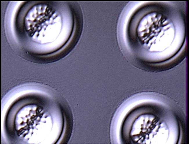
Inspection of surface underneath wafer with IR microscopy
Infra-red (NIR) Inspection of silicon wafer
IR microscopic inspection is normally carried out for silicon wafer when the structure that needs to be inspected is embedded beneath a layer of silicon. As silicon is transparent under the IR spectrum. We can see through the silicon to see the structure in IR. This make the structure that is otherwise impossible to see clearly visible and thus various inspection can be carried out. This method of inspection are widely used in MEMS production where wafers are very often bonded together.
Hard Disk Media Laser Bump Image with DIC observation
Inspection of hard disk media
In the centre of each hard disk is a disk media itself. The disk form the core of all data storage. We have vast experience in the inspection of disk media. The Nikon L200N and LV150N microscope is well suited for this application. The image on the right shows a media surface that is imaged with DIC which is one of the most important contrasting method for inspecting disk media. Apart from this, the newly designed TU series objective from Nikon has a much improved Dark Field which is also a very important tool in media isnpection.

Microstructure of metal for performing grain size measurement
Metallurgical Inspection / grain size inspection
Micro structure within a metal determines the property of the metal itself. With the Nikon MA100 and MA200 microscope coupled with metallurgical software, various analysis of the material can be done. The analysis is performed based on international standard such as ASTM, JIS, DIN, ISO etc. Various analysis can be readily done such as Grain Size measurement, Cast Iron analysis, Non Metallic Inclusion analysis etc. The picture on the right shows an image of metal with microstructure clearly shown.

Image of a Zebra fish embryo
Biological microscopy
In biological microscopy, the coverage is huge and wide from histopathology to cytology to live science imaging and sophisticated fluorescent imaging. Each area again has very stringent and specific requirement. The image on the right shows a zebra fish embryo. The research community has been working with zebra fish extensively to explore genetic expression via fluorescent after a modification of DNA has been done. We have been supplying Nikon microscope to the biological and research community since our founding.

Fracture surface of a metallic bolt
General stereoscopic microscopy
Stereo microscopes are generally used to inspect any surfaces that requires magnification of up to 200 times. The Nikon SMZ series of microscopes such as SMZ800N, SMZ1270, SMZ745 are all good tools for such application. Application are very wide, from inspection of PCB surfaces, to inspection of biological sample to inspection of fracture surfaces on metal. In the nut shell, if you need to see an item magnified but do not need ultra high magnification, then a SMZ series Stereo Microscope is suitable for you. The image on the right shows the fractured surface of a metallic bolt.


 Cell:+603 7987 3188
  Email: info@micro-optics.com.my
