InfraRed Microscopy
InfraRed Microscopy Inspection
InfraRed (IR) microscopic inspection is normally carried out for silicon wafer when the structure that needs to be inspected is embedded beneath a layer of silicon. As silicon is transparent under infra red. We can see through the silicon to see the structure in using IR. This make the structure that is otherwise impossible to see clearly visible and thus various inspection can be carried out. This method of inspection are widely used in MEMS production where semiconductor wafers are very often bonded together.
Wavelength used in IR microscopy
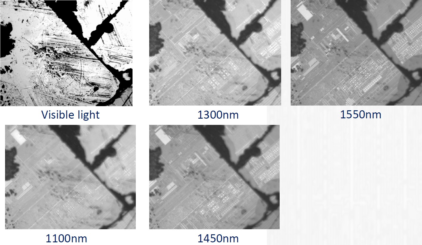
The most common and the lowest cost IR imaging method is using the 1100nm or below bandwidth. At this wavelength, lots of lenses and optics are still able to transmit this wavelength efficiently. Also, the commonly available CMOS NIR can be used for the imaging. Therefore, it is the cheaper option when it comes to IR imaging. However, there is a limit on what can be obeserved at 1100nm. This perhaps is due to the ability the wavelength is able to penetrate the silicon surface. In most case, much more detail can be observed at 1200, 1300, 1400 and 1500nm bandwidth. The problem is most lenses do not transmit wavelength above 1100nm. Therefore, in order for imaging to work at these bandwidth, special lense material, coating and processing needs to be done. Also, for detection of wavelength above 1100nm, InGaAs camera needs to be used. This leads to significantly higher cost. However, considering the additional detail that can be observed, most of the time, the higher cost is justified. Below is example of different images obeserved at different wavelength.
More images comparing image captured on CMOS and InGaAs camera at different wavelength

For the image on top, we compare images taken using CMOS IR camera with an InGaAs camera. Images are taken at 50X magnification (5X Objectives) at 1100nm and 1300nm. We can we that the images at 1300nm is significantly clearer. Also, although the CMOS IR camera can see some structures, they are not clearly visible. By far, image at 1300nm seems much better.
Images above are taken at 200X magnification. Similar observation as images taken at 50X magnification. Image is significantly better at 1300nm when using InGaAs camera.
Images above are taken at 500X magnification. Similar observation as images taken at 50X and 200X magnification. Image is significantly better at 1300nm when using InGaAs camera. We also obeserved that image from InGaAs camera at 1100nm is significantly under exposed. This may be due to the fact that InGaAs camera is not sensitive at wavelength below 1150nm.


